




ACS ami: Tunable p-Type Doping in Large-Scale MoS2 Films Realized by Selective-Area Gd Deposition
- 发布时间:
- 2026-07-14
- 文章标题:
- ACS ami: Tunable p-Type Doping in Large-Scale MoS2 Films Realized by Selective-Area Gd Deposition
- 内容:
https://doi.org/10.1021/acsami.6c01985
ACS 官方公众号:ACS ami 亮点速递
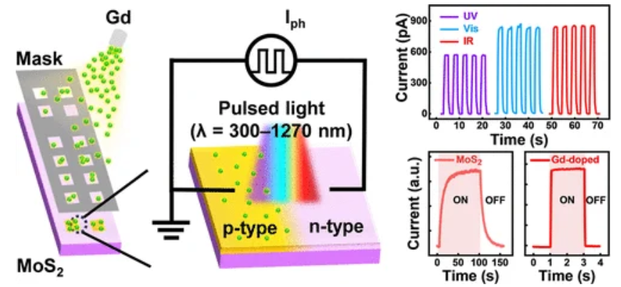
Self-powered ultralow energy consumption broadband optoelectronic devices based on two-dimensional (2D) semiconductor p–n junctions have emerged as a promising candidate for next-generation smart optosensors owing to the superior photoresponse driven by the intrinsic built-in electric field. However, efficient p-type doping remains a critical challenge for constructing high-performance devices. In this work, we developed a well-controllable doping procedure by ultrahigh vacuum (UHV) selective-area deposition and solid-state reaction, which has been applied in the tunable p-type doping of rare-earth metal Gd in large-scale MoS2 films. Scanning electron microscopy (SEM), X-ray photoelectron spectroscopy (XPS), and Kelvin probe force microscopy (KPFM) characterizations confirm uniform and effective doping in the selected area, with a 0.29 eV downward shift of the Fermi level induced by Gd substitution. Two terminal photodetection devices have been fabricated on the Gd-doped MoS2 lateral p–n homojunctions by using the shadow-mask-assisted patterned electrode deposition that guarantees atomically clean interfaces. Optoelectronic transport measurement under illumination of varying wavelengths revealed robust self-powered broadband photoresponse, featuring an open-circuit voltage of 38 mV at zero bias, as well as high responsivity (5.42 A/W) and detectivity (8.06 × 10¹¹ Jones) from the visible to near-infrared wavelengths range (300–1270 nm). In addition, the response speed has been improved by 3 orders of magnitude (from 104 ms to 20–50 ms) owing to the carrier recombination rate and mobility being enhanced by doping. Our work provides insights for the future advanced optoelectronic sensors of various 2D layered materials.
该论文近日发表在期刊ACS Applied Materials & Interfaces上,西安交通大学硕士研究生张旭涛,胡永琪,孙晓强,王浩等负责材料制备和性能测量,硕士生王连会负责真空沉积工艺;潘毅教授、张一诺博士为通讯作者,负责课题设计。