We are group of condensed matter experimentalists with interest in electronic properties of low-dimensional systems. Through state-or-art nano-fabrication and ultra-low noise low temperature electronic transport measurements, we aim to discover new phenomena and understand the underlying physics. We hope our work eventually will be relevant for applications, such as in sensing and in the storage of information. In the following, we show several examples of our research projects:
Magnetic Semiconductors (磁性半导体)
Two-dimensional (2D) magnetic semiconductors are an emerging class of materials that combine magnetism and semiconducting properties within atomically thin layers—something once thought to be incompatible. These materials allow us to control both the charge and the spin of electrons, offering a new platform for future spintronic and quantum devices. We demonstrated a nonvolatile and highly tunable magnetoresistance in hybrid spin filters, showing how spins can be manipulated to store and process information without energy loss. We reported magnetoresistance oscillations in the antiferromagnetic semiconductor—a surprising effect rarely seen in insulating systems—arising from the interplay between magnetic order and localized electronic states. Together, these findings reveal how 2D magnetic semiconductors can host new physical mechanisms beyond conventional magnetism and electronics, paving the way toward energy-efficient, spin-based technologies.

Reference:
Xiaoyu Wang, et al. “Large Tunneling Magnetoresistance in Nonvolatile 2D Hybrid Spin Filters” Physical Review Letters, 134, 077001 (2025)
P. Shi, et al. “Magnetoresistance Oscillations in Vertical Junctions of 2D Antiferromagnetic Semiconductor CrPS4” Physical Review X, 14, 041065 (2024)
L. Zhang, et al. “Bias voltage driven tunneling magnetoresistance polarity reversal in 2D stripy antiferromagnet CrOCl” Applied Physics Letters, 125, 222403 (2024)
Magnetism in two dimensions (二维磁性)
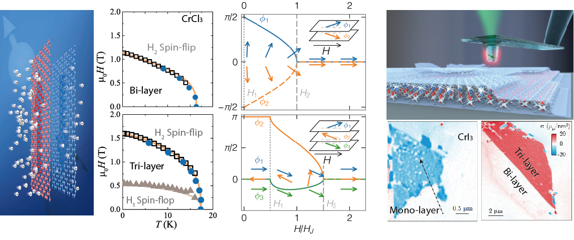
Long-range magnetic order in two dimensions has been at the heart of fundamental research in condensed matter physics, and is also crucial for future ultra-high density spintronic devices. However, experimental realization of two dimensional (2D) magnetism was extremely difficult until the successful isolation of first 2D magnet from van der Waals materials CrI3 in 2017. In our group, we mainly use electrical measurement methods to probe the magnetic properties of 2D magnets, reveal new phenomena and understand the underlying physics. For example, through tunneling magnetoresistance measurement, we determined the phase diagram of layered antiferromagnet CrCl3 and found interesting even-odd effect, we have demonstrated the persistence of magnetism in atomically thin MnPS3 crystals. In collaboration with other groups, we also investigate 2D magnetism with optical measurement methods, such as scanning single-spin magnetometry and magnetic circular dichroism.
Reference:
Z. Wang, et al. “Determining the phase diagram of atomically thin layered antiferromagnet CrCl3” Nature Nanotechnology 14, 1116-1122, (2019)
L. Thiel, et al. “Probing magnetism in 2D materials at the nanoscale with single-spin microscopy” Science 364, 973-976, (2019)
G. Long, et al. “Persistence of Magnetism in Atomically Thin MnPS3 Crystals” Nano Letters 20, 2452-2459 (2020)
N. Ubrig, et al. “Low-temperature monoclinic layer stacking in atomically thin CrI3 crystals” 2D Materials, 7, 015007 (2020)
2D spintronic devices (二维自旋电子器件)
Spintronic devices utilize spin instated of charge to store and process information, so that they can in principle offer low-power consumption and ultrafast speed. 2D materials are ideal candidates for fabricating ultra-high density spintronic devices, because 2D materials can be high quality even at atomically thin level and the interfaces of heterostructures can be atomically sharp. In our group, we are designing and fabricating different types of spintronic devices based on 2D materials, including classic magnetic tunneling junctions (MTJs) with ultra-thin barrier and new type of giant magnetoresistance devices constituted by multi-spin-filters.

Reference:
Z. Wang, et al. “Very large tunneling magnetoresistance in layered magnetic semiconductor CrI3” Nature Communications 9, 2516, (2018)
Z. Wang, et al. “Tunneling Spin Valves Based on Fe3GeTe2/hBN/Fe3GeTe2 van der Waals Heterostructures” Nano Letters 18, 4303-4308, (2018)
Quantum Transport in Graphene (石墨烯中的量子输运)
Graphene, a single layer of carbon atoms arranged in a honeycomb lattice, has become a fascinating platform for exploring quantum transport phenomena. My research focuses on bilayer graphene, where two layers can slide, twist, or be stacked in different ways, giving rise to tunable electronic states. By precisely controlling the stacking order and interlayer coupling, we discovered how sliding between layers can generate topological conducting channels, how quantum interference governs electron motion, and how symmetry breaking leads to new quantum phases. These findings deepen our understanding of electron behavior in 2D materials and point toward new strategies for designing low-dissipation electronic and quantum devices based on the topology of graphene layers.


Reference:
Jie Pan, et al. “Topological Valley Transport in Bilayer Graphene Induced by Interlayer Sliding” Physical Review Letters, 135, 126603 (2025)
J. Pan, et al. “Inducing Berry curvature dipole in multilayer graphene through inhomogeneous interlayer sliding” Physical Review B, 110, 235418 (2024)
Z. Wang, et al. “Strong interface-induced spin-orbit interaction in graphene on WS2” Nature Communications 6, 8339 (2015)
Z. Wang, et al. “Origin and magnitude of ‘designer’ spin-orbit interaction in graphene on semiconducting transition metal dichalcogenides”, Physical Review X, 6, 041020 (2016)